KVK Number: 98122312 Phone:+31 6 2889 0071 Email: fluxontechnology.bv@gmail.com
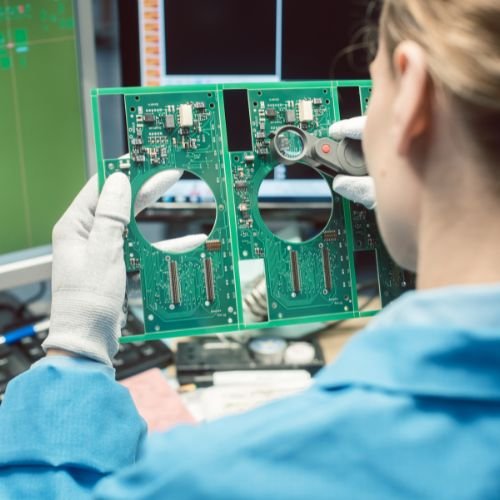
The printed circuit board serves as the foundation for modern electronics. It uses copper traces to connect electronic components while offering mechanical support and a compact form factor.
Early gadgets relied on point-to-point wiring and wire-wrapping, which proved bulky and less reliable. Boards replaced that approach by improving reliability, size, and manufacturability at scale.
At its core, each circuit board provides three roles: electrical interconnection, mechanical support, and a compact, manufacturable package for circuits.
Modern pcbs are multilayer stacks of copper and dielectric, protected by solder mask and labeled with silkscreen. Assembly mixes surface-mount and through-hole parts, and HDI design lets devices pack thousands of connections into phones, wearables, and servers.
In this guide, you will meet terms like traces, planes, vias, surface-mount parts, and through-hole components. Design choices—from layer stack to part placement—shape signal behavior, power delivery, thermal performance, and long-term reliability.
What is a PCB?
Circuit boards form the backbone of nearly every modern electronic device. They evolved from point-to-point wiring, then wire-wrap, into standardized printed wiring cards as parts shrank and integrated circuits rose.
Printed circuit board vs. printed wiring board: terminology and evolution
Printed circuit board, printed wiring board, and printed wiring card refer to the same basic idea. Over time, printed circuit became the standard term as circuits grew denser and manufacturing standardized.

Core functions: electrical interconnection, mechanical support, and compact form
A pcb uses copper patterns to route signals and power between components while the substrate gives structural support. This layered board holds parts in fixed positions for reliable connection and consistent performance.
- Accurate electrical paths for signals and power.
- Mechanical support for each component and mounting hardware.
- A compact package that meets device size and thermal needs.
Integrated circuits and modern packages pushed designers to adopt multilayer boards and denser routing. Substrate choice and stack-up affect rigidity, heat, and the final device function.
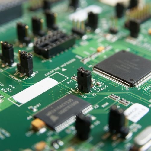
Inside a Circuit Board: Materials, Layers, and Copper Traces
Material choice and copper layout decide how well a board moves current and rejects noise. Designers pick substrates, layer count, and copper weight to meet thermal, mechanical, and signal goals.

Substrates and high-level materials
FR-4 fiberglass is the default rigid substrate because it balances cost, rigidity, and manufacturability for most boards. Flexible circuits use polyimide films for bendability and lower weight.
Ceramic and insulated metal substrate (IMS) options serve demanding thermal or mechanical needs, such as LED drivers or power modules.
Conductive features and copper choices
Traces route signals; pads hold component leads; planes distribute ground and power. Vias pass signals between layers, and choosing tented or exposed vias affects solderability and reliability.
Practical conversion: 1 oz/ft² ≈ 35 μm of copper. Higher weights (2–3 oz) support larger currents and better thermal spread.
Protective and identification layers
Solder mask prevents solder bridges and corrosion; color aids identification and branding but not electrical function. Silkscreen marks reference designators, polarity, pin‑1, and test points for quicker assembly and service.
| Material | Common Use | Strength | Example |
|---|---|---|---|
| FR-4 | Rigid boards | Good | Consumer electronics |
| Polyimide | Flex circuits | Flexible | Wearables |
| Ceramic / IMS | High-thermal | Very stiff/thermally conductive | Power modules, LEDs |
Types of Circuit Boards Used in Electronics Today
Different board constructions solve trade-offs between thermal handling, routing density, and flexibility.
Single-sided boards place copper on one face and suit low-cost consumer gadgets with few parts. Double-sided boards use both faces, which lets designers route more nets and add simple vias for interconnects.
Multilayer boards add internal layers for power and ground, offering controlled impedance and much higher component density. These boards help dense designs and high-speed circuits in compact devices.
Rigid, flexible, and rigid-flex options
Rigid boards are common for general electronics and networking gear. Flexible pcbs use polyimide for bendable interconnects in wearables and foldable devices.
Rigid-flex combines both, giving reliable fold points for aerospace and medical gear where space and durability matter.
Specialized boards and high-density options
Metal-core (IMS) and ceramic boards prioritize thermal paths for LED drivers and power modules. HDI supports fine-pitch parts and BGA fanout when integrated circuits push pin counts. UHDI or substrate-like pcbs use additive steps similar to IC substrates for ultra-small geometries.
- Pick single- or double-sided for cost and simplicity.
- Choose multilayer or HDI for density and signal control.
- Use flexible pcbs or rigid-flex where space and motion matter.
Choosing the right type balances cost, manufacturability, mechanical needs, and electrical requirements for modern devices.
From Design to Manufacturing: How PCBs Are Made
Manufacturing turns a board concept into a tested, ready-to-assemble part using precise imaging, lamination, and plating steps.
Inner copper layers start with photo imaging and subtractive etching to leave intended traces. Cores and prepregs then stack in the chosen sequence to meet impedance and power goals.
Subtractive and additive patterning
Traditional subtractive etching removes unwanted copper to form traces. UHDI and advanced boards can use additive deposition to build ultra-fine metal features and microvias beyond etching limits.
Stack-up, drilling, and plating
After lamination, accurate drilling creates via holes. Electroplating deposits copper inside holes to make plated through-holes and vertical interconnects between layers.
Finishing and testing
Solder mask protects copper and prevents shorts. Silkscreen adds reference marks for placement of components. Bare board electrical tests check continuity and isolation before assembly.
| Step | Key action | Why it matters |
|---|---|---|
| Inner-layer etch | Image and etch copper | Forms critical traces and planes |
| Lamination | Press cores and prepregs | Creates stable stack-up and impedance control |
| Drill & plate | Drill vias, electroplate | Enables layer-to-layer interconnects |
| Finish & test | Mask, silkscreen, bare-board test | Protects copper and verifies circuits |
Example timeline: inner-layer etch → lamination → drill/plate → outer image/etch → mask/silkscreen → test. Early DFM choices cut time, lower cost, and improve yield.
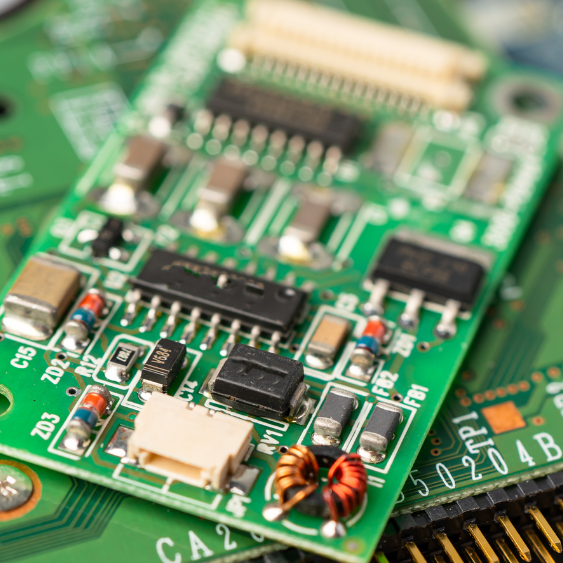
PCB Assembly Methods and Components
The methods used to attach parts define both manufacturability and long-term life of an electronic product. Choosing the right component style and solder process balances density, strength, and cost.
Through-hole vs. surface-mount
Through-hole parts provide sturdy mechanical anchoring and suit connectors, power terminals, and high-voltage or high-current points. They remain valuable when boards face mechanical stress.
Surface-mount devices let designers place components on both sides for much higher density. Modern pcbs use SMDs for most passive and IC parts to speed up automated placement and save time on assembly.
Assembly techniques: reflow, wave, pick-and-place
Standard SMT lines start with a paste stencil that deposits solder paste onto pads. Automated pick-and-place machines position components with high placement accuracy.
Reflow ovens use controlled thermal profiles to melt solder paste and form reliable joints. For through-hole work, wave soldering passes the board over molten solder, or selective soldering targets only specified areas when mixed technology is present.
Placement accuracy, paste volume control, and thermal profiling critically affect solder quality and yield. Inspection—automated optical inspection (AOI) and functional testing—validates workmanship before final test and shipping.
Good design choices—clearances, fiducials, panelization, and pick-and-place friendly footprints—cut assembly time, reduce errors, and lower production cost.
Stack-Up, Signal Integrity, and Power Integrity
A well-planned layer stack keeps signals clean and power stable as frequencies climb. Designers often start by dedicating internal layers to ground and power. This creates stable references for controlled impedance routing and helps reduce EMI.
Reference planes and EMI reduction
Solid ground and power planes give high-speed nets a predictable return path. That lowers loop area and cuts radiated emissions.
Continuous planes also make power distribution uniform, which keeps voltage rails steady under transient loads and helps sensitive circuits stay quiet.
Material selection for high-speed, high-reliability designs
Dielectric constant and loss tangent affect attenuation and impedance calculations. Low-loss laminates or PTFE substrates suit telecom and precision designs.
Thermal and mechanical properties matter for military and medical boards where reliability under stress is required.
| Material | Strength | Best use |
|---|---|---|
| FR-4 | Cost-effective, stable | Embedded designs and general boards |
| Low-loss laminate | Low attenuation | High-speed interfaces, telecom |
| PTFE | Very low loss, expensive | RF/microwave and precision signal work |
Practical guidance: start with a 4-layer stack (signal–GND–PWR–signal) for many embedded designs to balance cost and integrity.
Place decoupling networks near component power pins and stitch power planes with vias. Keep trace geometry and spacing aligned to the nearest reference plane to hit targets (50-ohm single-ended, 100-ohm differential).
Finally, minimize via transitions and stubs. Use breakout fanouts under fine-pitch packages and careful via planning under BGAs to preserve signal quality across the board.
Design Workflow and Tools in the Present-Day PCB World
Modern board development centers on tight feedback loops between engineers, ECAD tools, and fabricators. Teams begin with requirements, part selection, and schematic capture using validated libraries. Early stack-up planning sets impedance and layer targets before layout starts.
Front-end engineering and schematic capture
Engineers capture nets and power structure in schematics that link directly to footprints. Validated libraries reduce mistakes and speed procurement of components.
Placement, routing, and DRC: getting to a manufacturable design
Constraint-driven placement and routing enforce clearances, trace widths, and keep-outs. Automated DRC flags spacing, drill sizes, and annular ring violations so boards meet manufacturing limits.
Manufacturing deliverables: preparing files for fabrication and assembly
Before release, teams run design reviews and perform SI/PI or thermal simulation when needed. Final outputs include Gerber or ODB++, drill maps, stack-up notes, netlists, fabrication drawings, pick-and-place files, and paste layers.
“Aligning with your fabricator early reduces re-spins and speeds time to first articles.”
Version control and clear handoffs help global teams work across time zones and avoid costly errors. Early alignment on capabilities keeps prototypes predictable and production-ready.
Conclusion
Today’s electronic systems rely on careful board choices to turn schematics into reliable products. A printed circuit board gives dependable electrical connection and mechanical support so each device performs its intended function.
Materials, copper geometry, and stack decisions shape how circuits meet performance and EMI targets. Good design keeps parts and surface features arranged to aid assembly and long-term reliability.
The process moves from inner-layer etch and lamination to drilling, plating, finishing, and bare-board testing before assembly by reflow or wave soldering. Clear manufacturing rules make yields repeatable across consumer, industrial, medical, and aerospace devices.
Pick rigid, flex, rigid-flex, or specialized pcbs to match thermal and mechanical needs. Thoughtful plane use, decoupling, and routing keep power steady and signals clean over time.
Keep learning: smarter design and tighter collaboration with fabricators help teams deliver better electronics to the world.