KVK Number: 98122312 Phone:+31 6 2889 0071 Email: fluxontechnology.bv@gmail.com
Printed circuit board and PCBA often get mixed up in product talks. A printed circuit board refers to the bare substrate with copper traces that route signals. It carries vias, solder mask, silkscreen, and layered copper for complex routing.
PCB + components + soldering = PCBA sums the change. When resistors, capacitors, ICs, and connectors mount and get soldered, the board delivers real function in electronic devices like phones and automotive modules.
The journey starts with pcb design and fabrication — etching, drilling, plating, and panelization. Then assembly steps follow: solder paste printing, pick-and-place, reflow or wave soldering, and inspection with AOI or X-ray.
Why this matters: distinguishing circuit board from assembled boards shapes design choices, testing plans, and manufacturing timelines. Clear terminology shortens handoffs and improves product quality.

PCB vs PCBA at a glance: how a bare printed circuit board becomes a functional assembly
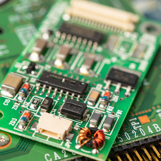
A bare board holds copper tracks and pads; adding parts turns it into a working circuit. The printed circuit substrate provides mechanical support and electrical interconnects. Testing at this stage checks continuity and finds shorts.
When components mount by SMT or THT and get soldered by reflow or wave, the board becomes a pcba ready for ICT and functional validation. Inspection often uses AOI and X-ray for dense packages like BGA.
Lifecycle in four steps
- Design & documentation: EDA outputs — Gerbers, BOM, pick-and-place.
- PCB fabrication: etch, drill, plate, mask, silkscreen, finish; drilled holes and vias enable layer connections and through‑hole parts.
- Assembly process: stencil printing, placement, reflow or wave soldering, inspection.
- Integration & deployment: system testing, field installation, ongoing support.
Manufacturing focus shifts: pcb quality centers on materials, layer registration, drilling accuracy, and plating. In contrast, pcbas demand precise placement, controlled reflow profiles, and strong solder joints. Use “pcb” when discussing stack-up and interconnects; use “pcba” when referring to ready-to-test assemblies.
What is a PCB? The printed circuit board as the foundation
A printed circuit board serves as the mechanical and electrical base that routes signals through laminated copper traces. The substrate gives rigidity or flexibility, depending on chosen material, while copper layers form the conductive paths that make circuits work.
The board stack-up normally includes substrate, one or more copper layers, a protective solder mask, and a silkscreen for assembly marks. Vias and plated-through holes connect internal layers and support through-hole parts.

Common materials and types
FR-4 is the go-to material for general electronics. Polyimide (Kapton) suits flex and rigid-flex designs. PTFE-based laminates serve high-frequency applications where low loss matters.
Design considerations
- Trace width and spacing control current and manufacturability.
- Layer count affects routing density; multilayer boards handle complex layouts.
- Controlled impedance keeps high-speed signals intact.
- Drill tolerances and via strategy impact yield and assembly reliability.
“Choosing the right stack-up and materials early saves time and reduces rework during production.”
| Feature | Best for | Material notes |
|---|---|---|
| Single/double-sided | Low-complexity, cost-sensitive designs | Standard FR-4, simple copper foils |
| Multilayer | High-density routing, signal integrity | Multiple copper layers, careful stack-up control |
| Flex / rigid-flex | Space-constrained or moving parts | Polyimide substrate, flexible copper |
| High-frequency | RF and microwave circuits | PTFE-based laminates for low dielectric loss |
Bare-board tests validate continuity and isolation before assembly. These checks reduce costly rework and ensure the board will support reliable manufacturing and performance.
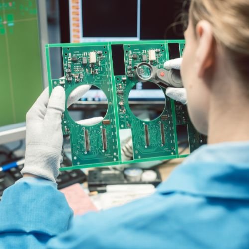
What is a PCBA? Turning a circuit board into a working device
Populating a bare board with parts and solder turns it into a functioning electronic module. This outcome — a pcba — pairs the printed substrate with mounted components and durable solder joints that enable operation.
Key assembly steps start with stencil printing of solder paste onto pads. Automated pick-and-place then positions SMDs for reflow. For through-hole parts, leads insert into drilled holes and get wave or hand soldering.
Paste deposition accuracy, pick-and-place alignment, and controlled thermal profiles determine joint quality and long-term reliability. SMT lines rely on tight tolerances; the assembly process documents profiles and timing to ensure repeatability.
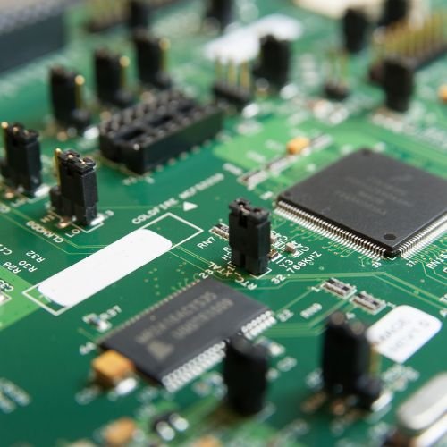
Inspection gates catch defects early. AOI flags misplacement and solder bridges. X-ray inspects hidden terminations like BGAs and QFNs with thermal pads.
Final test steps include ICT to verify nets and device-level functional tests before system integration. Clear sequencing, traceable documentation, and process control make reliable circuit board assembly repeatable at scale.
What is a PCBA? Definition, significance, and why it matters today
A finished assembly brings schematics to life by mounting parts and creating soldered connections that carry signals and power. Without assembly, a bare board stays inert. With components installed, the layout becomes a functional module ready for test and deployment.
How board assembly powers modern electronic devices
In smartphones, the mainboard pcba integrates CPU, memory, RF, and sensors to run apps and radio functions. In vehicles, pcbas power ECUs, safety systems, and infotainment. In medical equipment, assemblies follow strict workmanship and testing to meet safety standards.
Board-level integration concentrates performance: power delivery, signal conditioning, and compute sit on tight layouts that save space and weight. This enables wearables, networking gear, and compact industrial controllers.
- The pcba is the functional embodiment of a design that can be powered, programmed, and validated.
- Standards like IPC ensure repeatable quality across the industry.
- Reliable assemblies unlock modern applications across consumer and medical devices.
Assembly methods compared: SMT, through-hole, and mixed technology
Assembly choices shape final product performance, from tiny SMDs to rugged through-hole connectors.
Surface-mount benefits
SMT mounts SMDs directly on pads and uses reflow soldering for fast, automated placement. It enables high density and two-sided board assembly. This approach speeds production and suits compact electronics.
Through-hole strengths
Through-hole technology inserts components through drilled holes and often uses wave soldering. Use it when mechanical durability matters, for connectors, transformers, or parts with large leads that must withstand vibration.
Mixed-technology flows
Many products use mixed assembly: SMT handles small passives and ICs while THT supports heavy or high-current parts. Typical process routing: paste printing, SMT pick-and-place, reflow, THT insertion, wave or selective soldering, inspection, and test.
Inspection and testing
Quality checks include AOI for solder and placement, X-ray for hidden joints under BGAs, ICT to verify nets, and final functional tests. Component handling—moisture sensitivity, coplanarity, and thermal mass—affects soldering profiles and yields.
| Method | Strengths | Typical use |
|---|---|---|
| SMT | High density, fast automated placement, two-sided population | Mobile devices, networking, compact consumer boards |
| Through-hole | Mechanical strength, robust solder joints, resistant to vibration | Connectors, power modules, industrial controls |
| Mixed | Best of both: dense routing plus durable leads where needed | Products needing high performance and ruggedness |
| Inspection | AOI, X-ray, ICT, functional test ensure soldering quality | All board assembly lines before final acceptance |
Inside the manufacturing flow: from PCB fabrication to PCBA production
Manufacturing begins when copper patterns are transferred and layers are bonded into the final board stack. That initial work sets the electrical paths and mechanical base for later assembly.
PCB fabrication essentials: etching, drilling, plating, and panelization
First, the copper image is created by etching from Gerber artwork. Multilayer boards are then laminated, aligning each layer to maintain signal integrity.
Precise drilling makes vias and plated through holes that form interconnects and mounting points. Copper plating reinforces those holes and ties layers together.
Solder mask and silkscreen follow, and panels group multiple boards to speed manufacturing and reduce handling time.
PCBA process control: stencil printing, placement, reflow profiles, wave solder
On the assembly line, stencil printing deposits solder paste with tight volume control. Paste inspection and placement verification reduce placement faults.
Automated pick-and-place equipment offers high accuracy for small parts. Reflow ovens use controlled thermal profiles to ensure proper wetting and joint formation.
For through-hole parts, wave soldering or selective solder adds robust joints. Quality gates include bare-board electrical tests before parts are placed.
Key manufacturing metrics
| Stage | Control focus | Outcome |
|---|---|---|
| Fabrication | Pattern accuracy, layer registration, drill tolerance | Reliable copper traces and plated holes |
| Assembly | Paste volume, placement accuracy, oven profiling | Consistent solder joints and repeatable yields |
| Testing | AOI, X-ray, ICT, functional test | Early defect detection and lower DPMO |
| Operational KPIs | First-pass yield, throughput, DPMO | Line stability and cost per good board |
Design outputs such as Gerbers and drill files directly affect fabrication accuracy and yield. Clear documentation shortens setup time and lowers rework during assembly.
Design-to-manufacturing handoff: EDA files, DFM, and sourcing strategy
Clear documentation and vetted components cut down setup time and prevent line holds during first builds. Prepare Gerber layers, drill files, stack-up notes, and labeled BOMs so the factory can begin without back-and-forth.
EDA outputs and documentation
Deliver Gerbers, ODB++, drill maps, assembly drawings, and accurate pick-and-place coordinates. Include an approved parts list and footprint references.
Tip: Add component tolerances and moisture sensitivity data to avoid surprises during placement and reflow.
DFM and DFA essentials for better yields
Follow pad geometry, paste aperture, and keepout guidelines to reduce tombstoning and bridges. Use thermal reliefs and correct spacing to lower voids and soldering faults.
Early selection of compatible material and stack-ups helps signal integrity and downstream manufacturability.
Turnkey vs in-house assembly
Turnkey suppliers handle fabrication, sourcing, assembly, and test for speed and simplicity. In-house gives more control over process and parts but needs tooling and staffing.
Many teams choose a hybrid: outsource high-volume runs while keeping small runs or sensitive assemblies internal.
| Decision point | Consider | Outcome |
|---|---|---|
| Vendor selection | Certifications, equipment, test coverage | Lower risk, shorter ramp |
| Placement data | Accurate coords, polarity, fiducials | Fewer line stoppages |
| Revision control | Change logs, versioned files | Synchronized design and production |
“Well-prepared pcbs documentation accelerates NPI ramps and reduces re-spins.”
Real-world applications: where PCBs and PCBAs show up across industries
Across markets, circuit board assemblies enable compact, high-performance devices used every day.
Consumer electronics: smartphones, laptops, wearables
High-density pcbs with fine-pitch BGAs and multilayer routing power smartphone mainboards. Laptops and wearables use rigid and rigid-flex boards to stack processors, memory, and sensors into thin enclosures.
Key components here are processors, memory ICs, power stages, and tiny RF modules that drive functionality.
Automotive and industrial: ECUs, motor drives, PLCs
Automotive controllers mix SMT and through-hole for durability under heat and vibration. Heavy-copper boards carry higher currents in motor drives and power stages.
Serviceability and traceability shape design and production choices in this industry.
Medical, telecom, aerospace/defense: reliability and high-frequency needs
Critical systems demand controlled-impedance, high-layer-count printed circuit designs and RF laminates. Assemblies receive conformal coating or potting and go through rigorous testing for longevity.
- Cross-sector trend: higher density and miniaturization push advanced assembly and inspection.
- Material and stack-up choices support signal integrity and thermal performance at scale.
- Certifications and traceability ensure long-term service and regulatory compliance.
“Compact boards and precise assembly unlock the functionality modern devices require.”
Cost and lead-time drivers: PCB fabrication vs circuit board assembly
Cost and lead time shift quickly when design choices add layers, exotic material, or complex via work. Small changes at the fabrication stage ripple through manufacturing and the final assembly timeline.
Fabrication drivers that raise price and time
More layers, fine trace/space, and special laminates such as PTFE increase per-board cost. Blind and buried holes add drilling steps and alignment checks.
Thicker copper, tight impedance control, and exotic material choices demand extra inspection and slow down throughput.
Assembly factors that affect total cost
Board-level cost reflects BOM components, feeder setups, and mixed SMT/THT steps. AOI, X-ray, ICT, and functional testing add test time but cut returns.
Solder alloy selection and profile tuning influence first-pass yield and rework rates.
Scaling strategies for prototypes to production
Prototypes favor quick-turn pcbs and relaxed DFM. Low-to-mid volumes may use hybrid lines. For fast ramp, choose turnkey manufacturers to consolidate sourcing, assembly, and test.
“Standardize parts, align design rules with suppliers, and consolidate variants to lower cost and shorten lead times.”
Conclusion
Good documentation and stable processes turn designs into repeatable assemblies that meet field requirements.
Remember: a printed circuit board provides the substrate, copper interconnects, layers and vias. A pcba combines that board with components and soldering to become a working unit.
Keep the assembly process tight: clear BOMs, controlled solder paste and tuned smt placement reduce defects. Inspect with AOI/X-ray and run functional tests before shipment.
Next step: validate circuits with prototypes, tune paste and place parameters, and scale with manufacturers who match your surface assembly capabilities and industry expectations.
Track board quality metrics, refine parts and leads selection, and iterate designs. That discipline keeps devices reliable across applications.